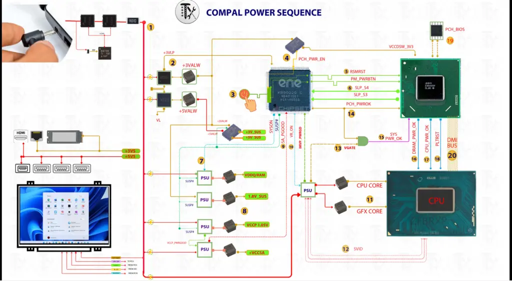
POWER SEQUENCE
⚙️ Overview of Haswell Power Architecture
Haswell CPUs (Intel 4th Gen Core i3/i5/i7) integrate the Fully Integrated Voltage Regulator (FIVR), which changes how power sequencing works compared to Ivy Bridge.
- Platform Controller Hub (PCH): Intel 8‑Series (HM86/HM87/Q87) manages system power states.
- Power Wells: PW1 (Always On), PW2 (Primary I/O), PW3 (Suspend).
- Key Rails:
- +3.3 V_AUX / +5 V_AUX → Always On (PW1)
- +3.3 V / +5 V / +VCC_CORE / +VCC_GT / +VCC_SA → Sequenced by EC and PCH logic
🔋 Compal Haswell Power‑Up Sequence (Simplified Flow)
| Step | Signal / Rail | Description |
|---|---|---|
| 1 | ACIN / ADP_PRESENT | Adapter detected; EC wakes from sleep. |
| 2 | +3.3 V_AUX / +5 V_AUX | Standby rails power EC, RTC, and PCH PW1. |
| 3 | EC_ON / SLP_S5# deasserted | EC enables main rails; system exits S5. |
| 4 | +3.3 V / +5 V main rails | Power to logic, USB, and PCH PW2. |
| 5 | SLP_S3# deasserted | Transition from S3 → S0; CPU VRs prepare. |
| 6 | VCC_CORE / VCC_GT / VCC_SA | CPU internal FIVR generates sub‑rails. |
| 7 | PCH_PWROK → CPU_PWROK | Confirms all rails stable; CPU begins execution. |
| 8 | PLTRST# deasserted | Platform reset released; BIOS starts POST. |
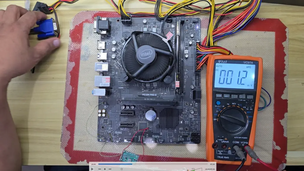
🧩 Diagnostic Notes for Board‑Level Repair
- Check EC_ON and SLP_S5# first when “no power” occurs.
- PCH_PWROK must go high before CPU VCC_CORE appears.
- VR_READY from the CPU VR controller signals FIVR readiness.
- VCCSA ≈ 0.9 V, VCCGT ≈ 1.05 V, VCCCORE ≈ 0.8–1.0 V depending on load.
- Resistance reference: CPU_CORE typically 2–10 Ω on Haswell mobile boards


Responses